Tag Archive for: Design

Company used for school website, software design finds ransomware in system


The company states it is “making significant progress to get all websites up and running” and that “full restoration has taken us longer than anticipated.” 

Finalsite took to its Facebook page Thursday to provide an update to its clients, saying an ongoing investigation shows as of this time, there is no evidence that data belonging either to the company, or its clients, has been taken.  

Source…

Inclusivity: The utilisation of design and ability – BCS


Inclusivity: The utilisation of design and ability  BCS

Source…

It’s time for tech to embrace security by design – TechCrunch


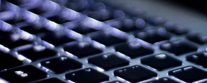
Cybercriminals are getting more and more adept at exploiting the latest trend or issue of high public interest to spread malware and steal personal data from unsuspecting users.

Whether it’s an app related to your favorite TV show, government health updates about COVID or tracking missed package deliveries, the result is too often the same: infected devices leading to fraud or outright theft.

Basic cybersecurity hygiene is the key to protecting your devices against the most common types of malware, but we also need security built into technology to prevent these sophisticated cyberattacks.

The Secret Service is certainly best known for protecting the president. But its other primary mission is to safeguard the nation’s financial infrastructure and payment systems to preserve the integrity of the economy from a wide range of financial and electronic crimes, including U.S. counterfeit currency, bank and financial institution fraud, illicit financing operations, identity theft, access device fraud and cybercrimes.

With the prevalence of mobile devices in today’s world, that means that, as the Department of Homeland Security (DHS) recommends, “users should avoid — and enterprises should prohibit on their devices — sideloading of apps and the use of unauthorized app stores.”

The pandemic has been a boon to cybercriminals, taking “advantage of an opportunity to profit from our dependence on technology to go on an internet crime spree,” said Paul Abbate, deputy director of the Federal Bureau of Investigation.

The FBI’s Internet Crime Complaint Center registered 791,790 complaints in 2020, nearly double the previous year’s total and the largest year-over-year increase ever recorded. One particularly insidious example was text messages that encouraged users to download an app to make vaccine appointments but then sent malware to every device in that user’s contacts that could steal personal data or banking information.

Earlier this year, the U.K.’s National Cyber…

Source…

NXP Semiconductors Selects AWS as Its Preferred Cloud Provider to Power Electronic Design Automation in the Cloud


SEATTLE–(BUSINESS WIRE)–Today, Amazon Web Services (AWS), an Amazon.com, Inc. company (NASDAQ: AMZN), announced that NXP Semiconductors N.V. has selected AWS as its preferred cloud provider and is migrating the vast majority of its electronic design automation (EDA) workloads from NXP data centers to AWS. Running on the world’s leading cloud extends NXP’s efficiency and competitive edge in the design and verification of advanced semiconductors tailored to the requirements of automotive, industrial Internet of Things (IoT), mobile, and communications infrastructure businesses. The Netherlands-based company uses AWS’s proven global infrastructure and capabilities in high performance computing (HPC), storage, analytics, and machine learning to enhance collaboration and EDA throughput across dozens of its worldwide design centers, as well as to reduce costs with elastic scaling of compute resources and minimize scheduling risks for design projects. In addition, thanks to AWS’s virtually unlimited scale, NXP engineers gain more time to focus on innovation rather than managing compute resources.

Running on AWS, NXP aims to achieve long-term process improvements that transform how semiconductors are designed and tested. Before NXP can manufacture new chips, its designs undergo extensive testing and validation through the EDA process to ensure they are functionally safe, secure, high quality, and highly performant. NXP’s complex EDA workflows include front-end design, performance simulation, and verification, along with backend workloads that include timing and power analysis, design rule checks, and other applications to prepare a chip for production. Historically, semiconductor companies run these highly iterative workflows from on-premises data centers with fixed compute capacity. However, because of the massive compute power involved for each cycle and the increasing complexity of chip designs, producing a new device can take many months or even years unless the companies accurately forecast and install additional compute infrastructure. In contrast, by powering its EDA with AWS, NXP gains the scale and agility to advance multiple projects at the same time on…

Source…